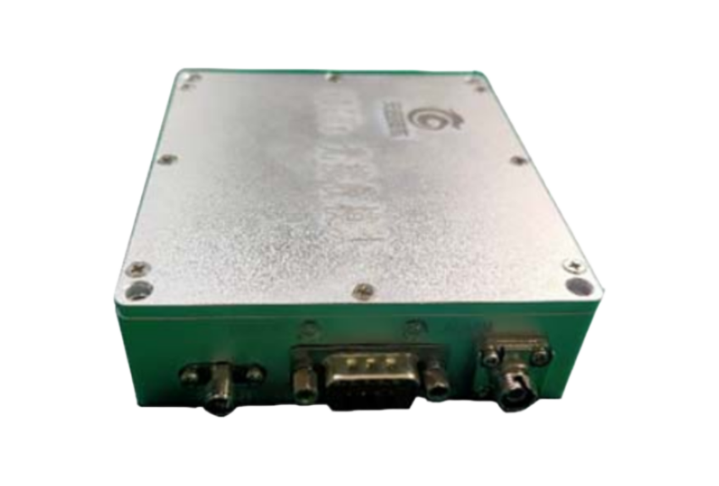
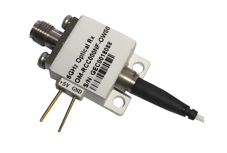
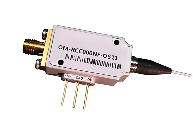
WXG45226Q Series 1GHz Balanced Photodetection Receiver Module
The WXG45226Q is a high-speed, high-sensitivity balanced-detector photoreceiver module that utilizes a monolithically integrated InGaAs balanced detector mixed with a low-noise transimpedance amplifier for a wide range of digital signal applications. Automatic detuning, gain, and bandwidth control provide stable bandwidth and output swing. The automatic gain control has a shutdown feature that provides a minimum gain of 400V/W after shutdown.
Model: wxg45226q
Applications:
RF over Fiber (ROF)
Wavelength:nm
Contact: Dongz
Email: Sales@wxgphotonics.com
Dongz
Email: Sales@wxgphotonics.com
Dongz
Email: Sales@wxgphotonics.com
Product Features
- InGaAs PD chip monolithic integration
- Integrated transimpedance amplifier circuitry
- Automatic gain and bandwidth control
- Supports 0.1 to 1Gbps rate AC differential outputs
- Hermetically sealed package, SSMA connector outputs
Applications
- DPSK/ DQPSK Optical Communication Systems
- Doppler Lidar Measurements
- Coherent Optical Systems
- High-speed test and measurement
Main performance index (Tc=22±3℃)
| Parameter name | Min | Typical | Max | Unit |
| Operating wavelength range λ | 1000 | — | 1650 | nm |
| Response Re | 0.8 | 0.84 | — | A/W |
| Differential conversion gain G | 400 | — | 8000 | V/W |
| 3dB Bandwidth f3dB | 1 | — | — | GHz |
| Common mode rejection ratio CMRR | 20 | 30 | — | dB |
| Saturated input optical power [1]PS | 10 | — | — | dBm |
| Optical Return Loss LO | 25 | — | — | dB |
| Low Frequency Cutoff Frequency LFC | — | 15 | — | kHz |
| Equivalent noise power density NEP | — | — | 10 | pW/Hz1/2 |
| PD dark current ID | — | — | 20 | nA |
| Differential output swing OS | — | 200 | — | mVpp |
| TIA Operating Current ICC | 30 | 40 | 50 | mA |
Note [1]: Saturation input optical power is detector chip saturation optical power;
Note: Test conditions VPD+=5V, VPD-=-5V, VCC=3.3V, λ=1.55μm.
Absolute Maximum Ratings
| Parameter name | Rating | Unit | |
| Storage temperature range TSTG | -40 ~ +85 | ℃ | |
| Operating Temperature Range TC | -20 ~ +50 | ℃ | |
| PD Bias Voltage | VPD+ | 5.2 | |
| V | |||
| VPD- | -5.2 | ||
| Amplifier Bias Voltage VCC | 3.6 | V | |
| Balanced input optical power Pin_B | 8 | mW | |
| Single-ended input optical power Pin_S | 1 | mW | |
| welding temperature Tp | 260(10s) | ℃ | |
| Electrostatic discharge sensitivity | ≥250 | V | |
| Minimum Bend Radius of Optical Fiber | 20 | mm | |
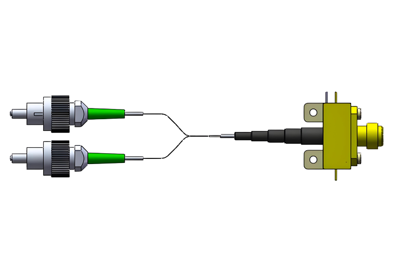
Package Outline, Dimensions and Pin Definition (Unit: mm)
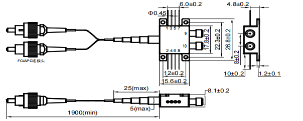
Lead Definition
| Lead-in number | Function | Lead-in number | Function |
| 1 | GND | 6 | VAGC |
| 2 | GND | 7 | GND |
| 3 | VPD+ | 8 | GND |
| 4 | VPD- | 9 | RF OUT+ |
| 5 | VCC | 10 | RF OUT- |
Product Inquiry
Leading manufacturer of photodetector modules and fiber optic sensing system modules